- Chuck Clean Wafer (CCW) | Wafer Chuck Cleaning Sol
- Features & Benefits
- Compatible Equipment & Usage Records
- Selection & Contact
Chuck Clean Wafer
Wafer Chuck Cleaning Solution
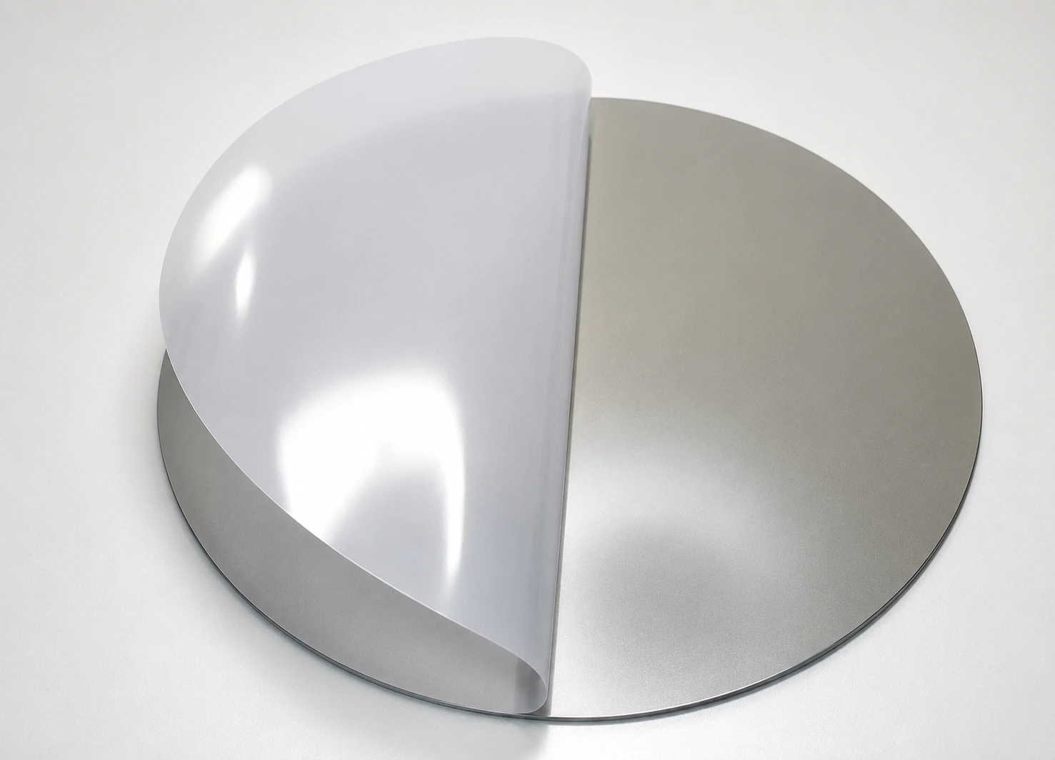
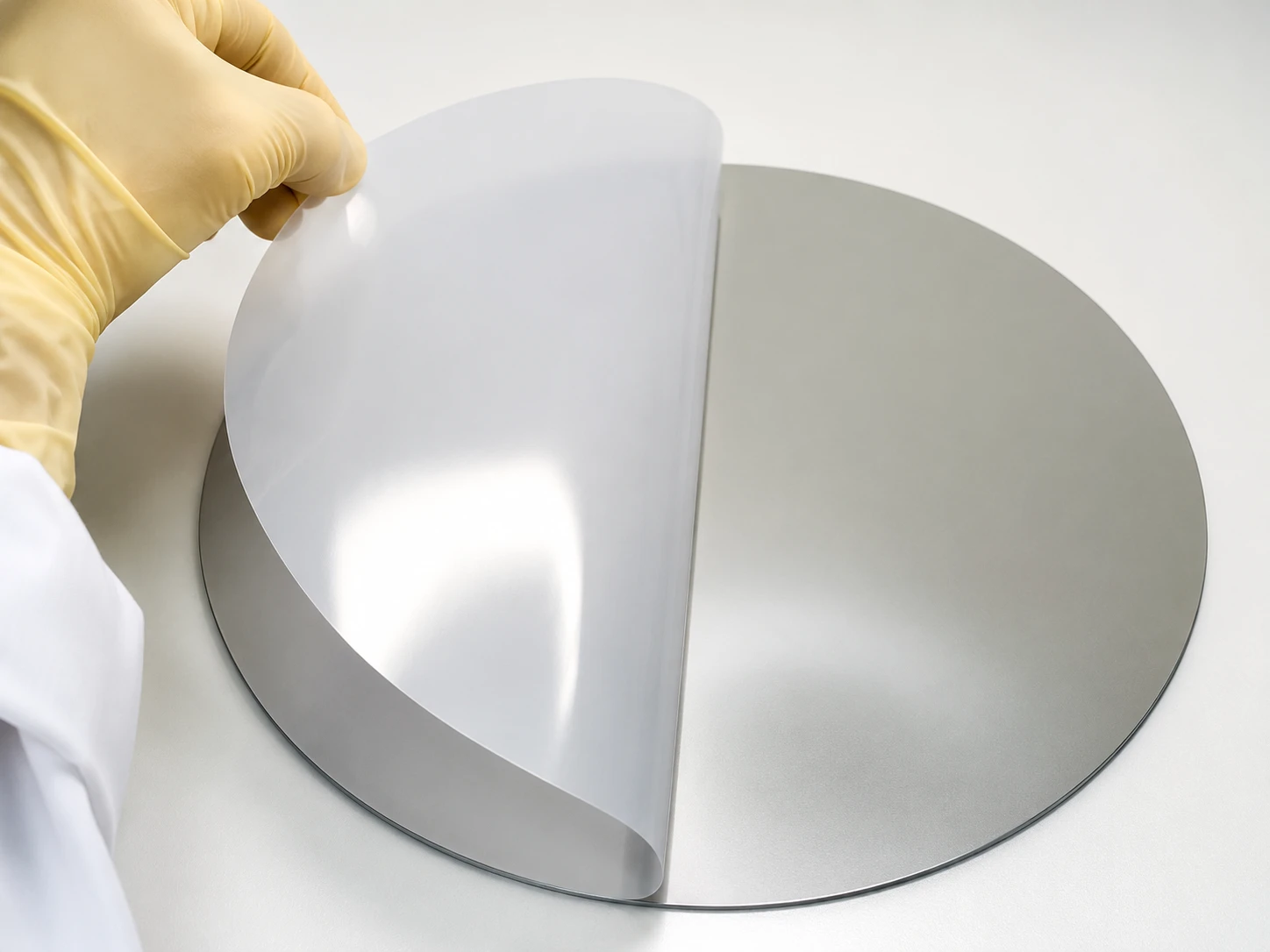
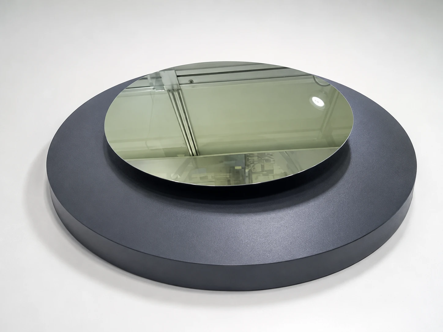
Chuck Clean Wafer is a cleaning wafer designed to remove particles and contaminants from wafer chuck surfaces in semiconductor manufacturing equipment.
The product is based on a silicon wafer coated with a proprietary polymer film. By transferring the wafer through the equipment in the same manner as a process wafer, particles on the chuck surface can be removed through the tack and adsorption characteristics of the cleaning layer.
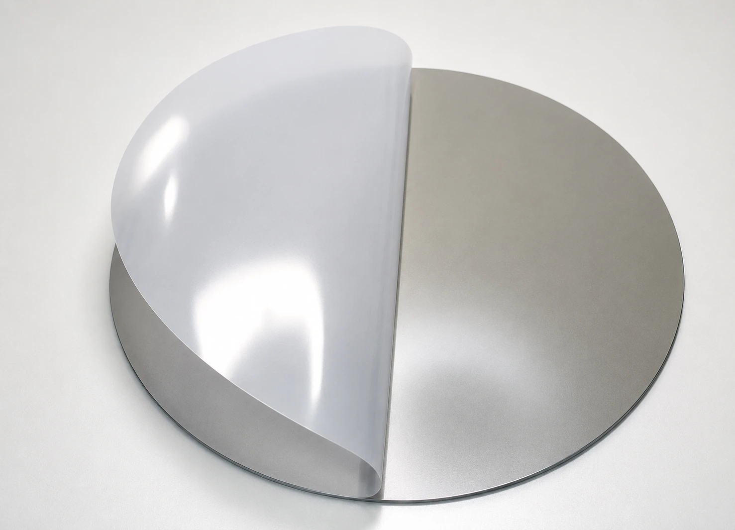
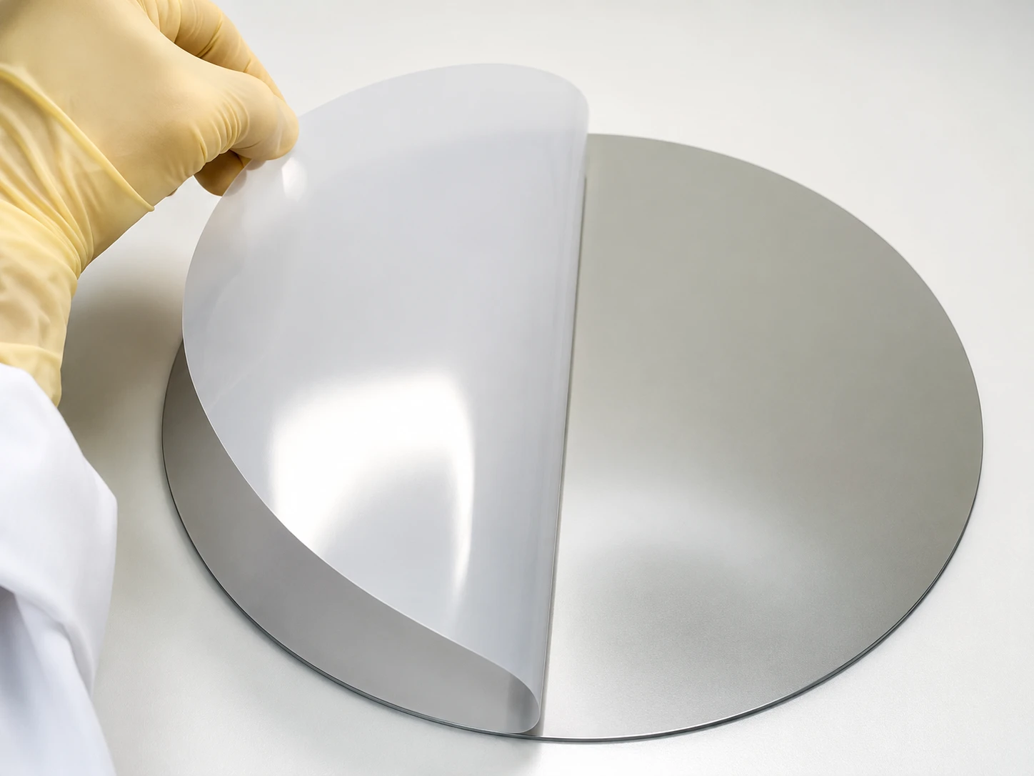
Product Structure
Chuck Clean Wafer uses a silicon wafer as the base material. A proprietary polymer cleaning layer is applied to the wafer surface, allowing contaminants on the wafer chuck to be picked up during equipment transfer and contact.
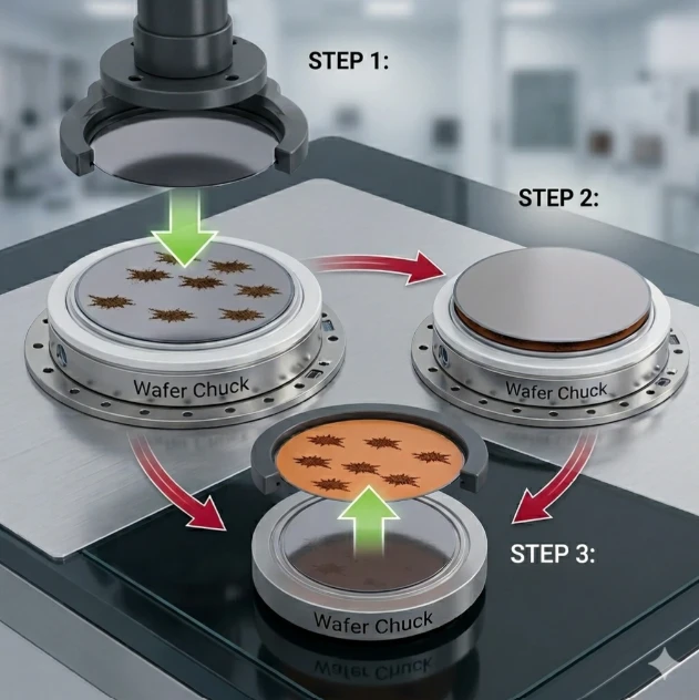
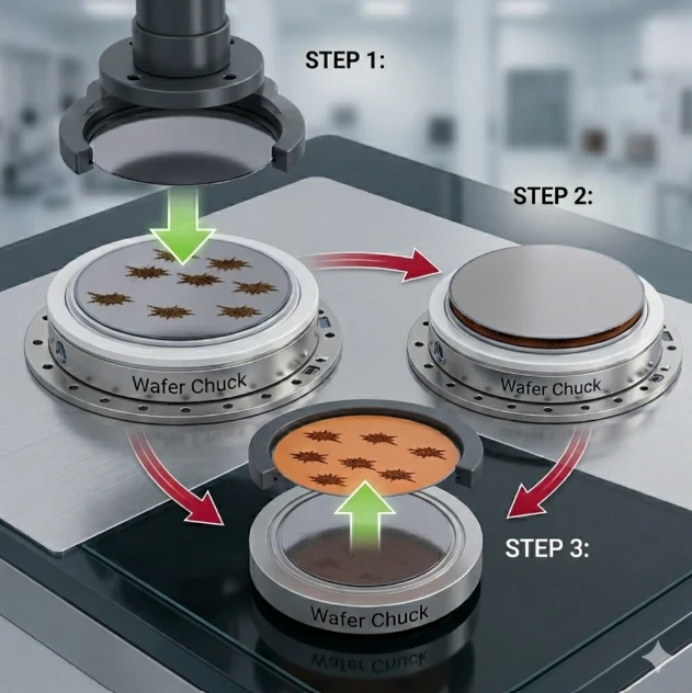
How Chuck Clean Wafer Cleans the Wafer Chuck
STEP 1|Load and Transfer
Chuck Clean Wafer is transferred into the equipment through the normal wafer handling sequence.
STEP 2|Contact with the Wafer Chuck
The cleaning surface comes into contact with the wafer chuck. Particles and contaminants on the chuck surface adhere to the cleaning layer.
STEP 3|Unload
The wafer is removed from the chuck, carrying the collected particles away from the chuck surface.
Cleaning Without Direct Manual Access to the Chuck
Because Chuck Clean Wafer can be transferred through the equipment automatically, the wafer chuck can be cleaned by using the equipment's wafer handling sequence. This provides a practical cleaning option for removing particles and contaminants from chuck surfaces inside semiconductor manufacturing equipment.
Applicable Semiconductor Processes
・CVD
・PVD
・ETCH
・PHOTO / Photolithography
・PROBER
Chuck Clean Wafer at a Glance
・Silicon wafer-based cleaning product
・Proprietary polymer cleaning layer
・Designed for wafer chuck particle removal
・Compatible with automatic wafer transfer
・Applicable to multiple semiconductor processes
・Available for equipment evaluation based on wafer size and tool configuration
※ Actual compatibility depends on wafer size, equipment model, chuck configuration, process conditions, and operating environment. Please provide your equipment information for compatibility and product selection evaluation.
Chuck Clean Wafer|Features & Benefits
Chuck Clean Wafer provides a wafer-based cleaning method for removing particles and contaminants from wafer chuck surfaces. By utilizing the equipment's wafer handling sequence, Chuck Clean Wafer can be transferred to the chuck without direct manual cleaning of the chuck surface.
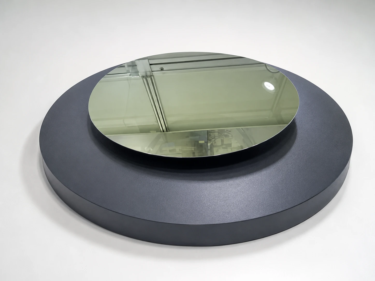
01|Compatible with Automatic Wafer Transfer
Chuck Clean Wafer is designed to be transferred through semiconductor manufacturing equipment using the equipment's wafer handling sequence. This allows the cleaning wafer to reach the wafer chuck without direct manual access to the chuck surface.
02|Particle and Contaminant Removal
The proprietary polymer cleaning layer uses tack and adsorption to pick up particles and contaminants from the wafer chuck surface when the cleaning wafer contacts the chuck.
03|Reduced Manual Chuck Cleaning
Because Chuck Clean Wafer can be introduced through the normal wafer transfer path, it provides an alternative cleaning method for situations where direct manual access to the wafer chuck is inconvenient.
04|Supports More Efficient Cleaning and Maintenance
Using a wafer-based cleaning method can help simplify chuck cleaning operations and reduce the amount of direct cleaning work required during equipment maintenance.
05|Applicable to Multiple Semiconductor Processes
Chuck Clean Wafer can be evaluated for use across multiple semiconductor manufacturing processes, including CVD, PVD, ETCH, PHOTO / Photolithography, and PROBER applications.
06|Evaluation Based on Wafer Size and Tool Configuration
Product selection and compatibility can be evaluated based on wafer size, equipment model, chuck configuration, process conditions, and operating environment.
Key Benefits
・Wafer-based chuck cleaning method
・Particle and contaminant removal by tack / adsorption
・Compatible with automatic wafer handling
・Reduced need for direct manual chuck cleaning
・Applicable to multiple semiconductor processes
・Compatibility evaluation based on equipment and wafer conditions
※ Actual cleaning performance and compatibility depend on wafer size, equipment model, chuck configuration, process conditions, contamination condition, and operating environment. Please contact KJT for evaluation based on your equipment information.
Chuck Clean Wafer|Compatible Equipment & Usage Records
Chuck Clean Wafer has been used with semiconductor manufacturing equipment across multiple wafer sizes and process applications. Compatibility should be evaluated based on the specific equipment model, wafer size, chuck configuration, and operating conditions.
Applicable Processes
・CVD
・PVD
・ETCH
・PHOTO / Photolithography
・PROBER
Equipment Usage Records
The following are representative equipment usage records for Chuck Clean Wafer.
| Wafer Size | Process | Equipment / Model |
|---|---|---|
| 150 mm | LITHO | CANON |
| 200 mm | PVD | AMAT ENDURA |
| 200 mm | ETCH | TEL UNITY |
| 300 mm | PVD | AMAT ENDURA |
| 300 mm | ETCH | LAM KIYO |
| 300 mm | LITHO | ASML |
| 300 mm | CVD | AMAT Producer SE |
| 300 mm | CVD | TEL Trias |
Wafer Size Experience
Usage records include 150 mm, 200 mm, and 300 mm wafer platforms. Actual availability and compatibility should be confirmed based on the target equipment and chuck configuration.
Equipment Brands in Usage Records
・Applied Materials (AMAT)
・Tokyo Electron (TEL)
・Lam Research (LAM)
・ASML
・Canon
Compatibility Evaluation
Even when the equipment brand or model is listed above, actual compatibility may vary depending on wafer size, chuck structure, equipment configuration, process conditions, and wafer handling sequence. Please provide the target equipment information for evaluation.
※ The above table shows representative usage records and does not guarantee compatibility with every configuration of the listed equipment. Final product selection should be confirmed based on the actual tool and operating conditions.
Chuck Clean Wafer|Selection & Contact
Chuck Clean Wafer selection and compatibility should be evaluated based on the target semiconductor equipment, wafer size, process application, chuck configuration, and operating conditions.
To help KJT evaluate the appropriate cleaning wafer for your equipment, please provide as much information as possible about the current tool and application.
Information for Product Selection
01|Equipment Manufacturer
Please provide the manufacturer of the target semiconductor equipment.
02|Equipment Model
Please provide the equipment model or tool name whenever available.
03|Process Application
Please specify the applicable process, such as CVD, PVD, ETCH, PHOTO / Photolithography, or PROBER.
04|Wafer Size
Please provide the wafer size used in the equipment, such as 150 mm, 200 mm, or 300 mm.
05|Chuck / Stage Information
If available, please provide information about the wafer chuck or stage configuration, including photos or relevant specifications.
06|Current Cleaning Issue
Please describe the current issue, such as particles or contaminants observed on the chuck surface.
07|Operating / Process Conditions
Please provide any relevant operating or process conditions that may affect product selection or compatibility.
Chuck Clean Wafer Selection Process
| STEP 1 | Provide equipment manufacturer, model, process, and wafer size. |
| STEP 2 | Confirm chuck configuration, wafer handling conditions, and current cleaning requirements. |
| STEP 3 | KJT evaluates Chuck Clean Wafer compatibility and product configuration for the target equipment. |
| STEP 4 | Recommended Chuck Clean Wafer specifications and evaluation conditions are proposed based on the available equipment information. |
Reference Applications
Chuck Clean Wafer usage records include equipment in the following process areas:
・CVD
・PVD
・ETCH
・PHOTO / Photolithography
・PROBER
Reference Wafer Sizes
Existing usage records include 150 mm, 200 mm, and 300 mm wafer platforms. Compatibility for each individual tool should be evaluated separately.
Looking for a Chuck Cleaning Solution for Your Equipment?
Please provide your equipment manufacturer, model, wafer size, process application, and current chuck cleaning issue.
KJT will review the available information and evaluate an appropriate Chuck Clean Wafer solution.
※ Actual product selection and compatibility depend on equipment model, wafer size, chuck configuration, wafer handling sequence, process conditions, contamination condition, and operating environment. Compatibility should be confirmed for the specific target equipment before use.